Your first cell: an inverter from schematic to LVS
In this tutorial you design a CMOS inverter on SKY130 from an empty library to a layout that passes DRC and LVS. You work in the browser the whole way, and the steps that a script can do for you name that script.
When you finish, the library invlib has:
- a cell
invwith a schematic (one pfet, one nfet, portsA,Y,VDD,VSS), a symbol and a routed layout; - a testbench
tb_invthat drivesinvwith a pulse and loads it with 20 fF, and its transient run in ngspice; - a spec in the cell's intent, "falling delay at most 100 ps", measured on that testbench;
- clean DRC and a matching LVS, and a cell page that says the schematic, symbol and layout agree and the checks pass.
Before you start
You need:
- Undine installed with the sky130A PDK and its tools (ngspice, KLayout, Magic, Netgen). See
Install.
./setup.sh check(orpixi run doctor) tells you what is missing. -
A project on sky130A. This tutorial uses the project
demofrom First project. If you do not have it yet, create it:pixi run python -m undine new demo --pdk sky130A -
The server running, with MCP on. You need MCP only for the
undine callcommands (step 7, and the optional one in step 5); every browser step works without it.UNDINE_MCP=1 pixi run serve # http://127.0.0.1:8700
Open http://127.0.0.1:8700 and choose demo in the project menu at the top left.
Why a new library?
If you did First project, demo already has the library mylib with a finished inv, its testbench tb_inv and
the Tiny Tapeout tile tt_um_undine_inv, which places that inv. This tutorial builds everything in a library of
its own, invlib, so it does not clash with those cells or draw over the one the tile uses.
Short on time?
Two scripts build the same cell. The steps that a script covers (steps 1 to 4, 8 and 9) have a Command line tab that names it; the other steps are the same on both paths. You can skip the drawing and still follow the rest in the browser:
pixi run python examples/make_inverter.py demo invlib     # schematic inv, symbol, testbench tb_inv
pixi run python examples/route_inverter.py demo invlib    # layout of inv: generated, routed, then LVS
Run them on the machine where the server runs, with the same UNDINE_ROOT: make_inverter.py writes the files
straight into the project directory; route_inverter.py works through the server's HTTP API and also reads the
saved layout files.
1. Create a library and a cell
- In the library browser on the left, click the folder button (New library). Enter
invliband click Create. The library appears under Project libraries. - Point at the
invlibrow and click + (New cell (schematic, symbol, layout)). - Enter
invas the Cell name. Leave Schematic ticked under Views and click Create.
The schematic editor opens on an empty sheet, with a tab invlib/inv. The library browser shows inv with a
sch badge.
examples/make_inverter.py creates the library if it does not exist, then writes inv.sch, inv.sym and
tb_inv.sch into it. It covers steps 1 to 4:
pixi run python examples/make_inverter.py demo invlib
It prints one wrote ... line per file. Reload the browser to see the cells.
2. Draw the schematic
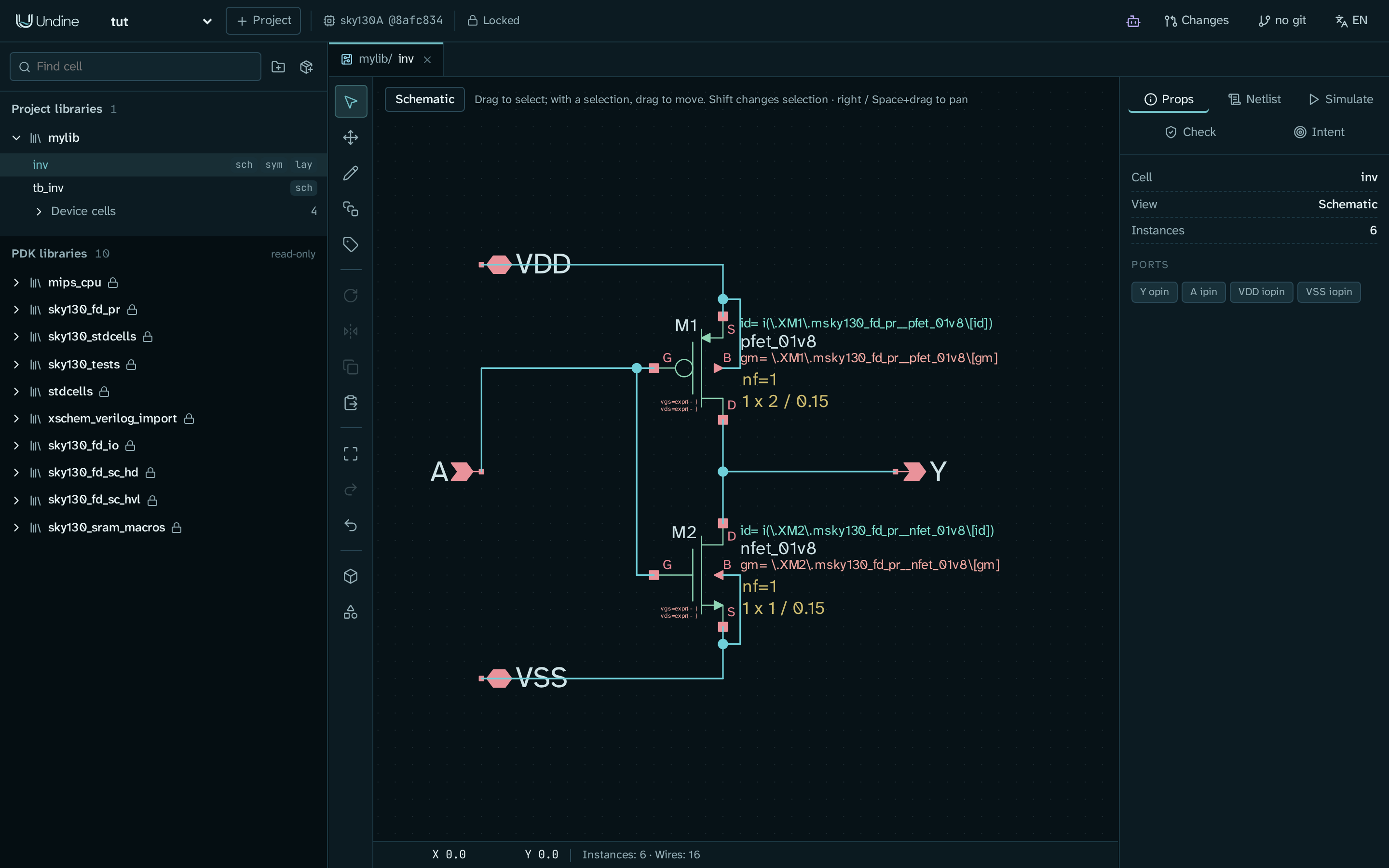
The inverter is two transistors between the supplies, with their gates joined (input A) and their drains joined
(output Y).
Place the transistors.
- Press I (or click Place symbol (I) in the toolbar). In the picker, type
pfet_01v8and clickpfet_01v8(librarysky130_fd_pr). - Click on the sheet to place it, then press Esc. It is named
M1. - Do the same with
nfet_01v8and place it belowM1. It is namedM2. - Click
M1. In the Props tab on the right, setWto2and press Enter. LeaveLat0.15. The pull-up is twice as wide as the pull-down because holes are less mobile than electrons; the wider pfet roughly balances the rising and falling edges.
Place the ports. Ports are the symbols ipin, opin and iopin of the devices library. Type pin in the
picker to see them. Place them in this order, because the order you place the ports in is the cell's port order:
| Port | Symbol | Where |
|---|---|---|
A |
ipin |
left of the gates |
Y |
opin |
right of the drains |
VDD |
iopin |
top left |
VSS |
iopin |
bottom left |
Each new port is called xxx. Click it and set its lab attribute in Props to the port name. The Ports
list of the schematic's properties (click empty space) then shows A ipin, Y opin, VDD iopin, VSS iopin.
Wire it. Press W for the wire tool. Click a pin to start a wire and another pin, or an existing wire, to finish it. The router draws the bends and goes round the device bodies. Draw these connections:
Ato the gate (G) ofM1, and the gate ofM2to the gate ofM1;- the drain (
D) ofM1to the drain ofM2, andYto that wire; VDDto the source (S) ofM1, and the body (B) ofM1to its source;VSSto the source ofM2, and the body ofM2to its source.
Press Esc when you are done. A dot marks each T junction. The status bar shows Instances: 6 · Wires: ....
Edits are saved to inv.sch as you make them; there is no save step. Details of every tool are in the
Schematic editor guide.
make_inverter.py (step 1) already wrote this schematic, with the same devices, sizes and ports.
Check the netlist. Open the Netlist tab on the right. You should see a subcircuit with your four ports and the two transistors:
.subckt inv A Y VDD VSS
XM1 Y A VDD VDD sky130_fd_pr__pfet_01v8 L=0.15 W=2
...
XM2 Y A VSS VSS sky130_fd_pr__nfet_01v8 L=0.15 W=1
...
.ends
If the ports come in another order, you placed them in another order; you can still follow the tutorial, and the
symbol's pins follow the same order. If a transistor lists a net such as net1 where you expected a port name, a wire
does not reach its pin: draw it again.
3. Make the symbol
A testbench places the inverter through its symbol.
- In the schematic's toolbar, click Create symbol from schematic (the button near the bottom of the toolbar).
- The symbol editor opens on a box with
Aon the left andY,VDDandVSSon the right. The side panel lists Pins in netlist order:A(Input),Y(Output),VDDandVSS(Input / output). - Go back to the
invschematic, open the Check tab and click Check schematic / symbol. You should see Interfaces match.
You can move the pins and draw a nicer outline (P pins, L lines, B boxes); see Symbol editing.
make_inverter.py wrote inv.sym, a square with A on the left, Y on the right and the supplies on top and
bottom.
4. Build a testbench
A testbench is a schematic that places the cell and drives it. It has no ports of its own.
- Create a cell
tb_invininvlibwith a schematic, as in step 1. - Press I and place:
inv(libraryinvlib): your inverter, namedx1;- two
vsourcesymbols: the supply and the input; - one
capa: the load; - a
gndat the bottom pin of each source and of the capacitor, and one more for the inverter'sVSS.
-
Click each part and set its attributes in Props:
Part namevaluesupply source Vdd1.8input source Vinpulse(0 1.8 1n 100p 100p 5n 10n)capacitor CL20f -
Connect the nets with labels instead of wires. Click Place net label (L), enter the Net name and click Place, then click each pin that belongs to the net. Press Esc before the next name.
in: the top pin ofVinand pinAofx1;vdd: the top pin ofVddand pinVDDofx1;out: pinYofx1and the top pin ofCL.
Labels with the same name are one net. Press X while placing to mirror a label on a right-hand pin.
-
Draw a wire from pin
VSSofx1to itsgnd.
make_inverter.py wrote tb_inv.sch with the same sources and load. It also has a code block with the model
library and its own .control script (tran 20p 20n), so you can run it with Use commands in the schematic in
the next step.
Check the netlist. Open the Netlist tab of tb_inv. Above the .subckt inv of step 2 you should see the
inverter and the three parts on the nets in, out, vdd and 0 (ground), in the order you placed them:
x1 in out vdd 0 inv
Vdd vdd 0 1.8
Vin in 0 pulse(0 1.8 1n 100p 100p 5n 10n)
CL out 0 20f m=1
A net such as net1 in one of these lines means that a label or a gnd does not touch its pin: delete it and place
it again on the pin's end.
5. Run a transient simulation
- In
tb_inv, open the Simulate tab on the right. - Set Analysis to Transient (.tran). Set Step to
20pand leave Stop at20n. - Click Run ngspice.
The run appears under Jobs and takes well under a second. When it is done, the plot shows v(in), v(out) and
v(vdd). Untick v(vdd) in the signal list, then scroll on the plot to zoom in on the input's rising edge at 1 ns:
v(out) falls a few tens of picoseconds after v(in) crosses 0.9 V. Double-click the plot to zoom out again.
Where the transistor models come from
Your testbench has no model statement, so Undine includes the PDK's typical corner (tt) and says so in the job.
To choose another corner, place the PDK's corner symbol sky130_fd_pr/corner.sym in the testbench; see the
Schematic editor guide. How the models are loaded is in
PDK models in a simulation.
A testbench you drew this way has no .control block, so the analysis you set in the panel is what runs. A testbench
with its own .control block (the one from make_inverter.py) runs as written with Use commands in the schematic.
From the shell, with MCP on, run_simulation does the same run. Pass the analysis as JSON (key:=json): without it,
only the schematic's own .control block runs, and your testbench has none.
pixi run python -m undine call run_simulation lib=invlib cell=tb_inv 'analysis:={"type":"tran","step":"20p","stop":"20n"}' --project demo
The result says "analysis": "Transient Analysis" and summarises each signal.
6. Record what the cell has to do
Each cell has a design intent: its goals, preferences, constraints and specs, each with why. Undine's flow steps read it, and so does an AI agent working on the cell. Here you describe the ports and add one spec.
- In the library browser, click the name
inv(not a badge). The cell page opens. It says In invlib. Its schematic and symbol agree. and lists the views, withtb_invas a Testbench that places inv. - Click Edit intent.
-
Under Ports, set each port's Kind and Side:
Port Kind Side Asignal in W Ysignal out E VDDsupply N VSSground S -
Under Supplies, click Use suggested supplies. The editor now shows Ready for simulation and Ready for layout.
-
Under Add to the intent, choose Spec and fill in:
- the text:
Falling delay at most 100 ps into 20 fF; - Measure:
tphl; - Max:
1e-10(the form takes a plain number, in seconds); - Testbench:
tb_inv; - Why:
it drives the next stage at 100 MHz.
Click Add. The spec appears under Specs as
s1,tphl ≤ 1e-10 (tb_inv). - the text:
-
The spec still has to say how
tphlis measured. Click YAML and add the linesanalysisandmeasundertestbench: tb_inv, at the same indentation, so that the spec reads:spec: measure: tphl max: 1.0e-10 testbench: tb_inv analysis: {type: tran, step: 20p, stop: 20n} meas: ".meas tran tphl trig v(in) val=0.9 rise=1 targ v(out) val=0.9 fall=1"analysisgives the spec's runs their transient, since your testbench has no.controlblock of its own (a spec on themake_inverter.pytestbench can leave it out).measis the.measstatement that definestphl: the time fromv(in)rising through 0.9 V tov(out)falling through 0.9 V.Click Save YAML, then Form to go back. The
.measstatement is added to the spec's own runs only; the testbench file does not change.
Click Close the editor. The cell page now lists the spec under What it has to do, says
Ready for simulation and layout., and shows tb_inv as a testbench that measures s1.
The intent is stored next to the cell, in libs/invlib/inv.intent.yaml of the project. The kinds of item and the
intent editor are in Cells, intent and views and the design document; what
a spec can measure, and its analysis and meas, are in the Specs paragraph of
The tool surface.
7. Measure the spec
The browser records specs; the measuring is done by the check_specs tool, which an AI agent calls and you can call
from the shell. It needs the server running with MCP on (see Before you start).
pixi run python -m undine call check_specs lib=invlib cell=inv --project demo
The result lists each spec with its status, its worst value and the margin to the limit:
{
  "specs": [
    {
      "id": "s1",
      "text": "Falling delay at most 100 ps into 20 fF",
      "measure": "tphl",
      "min": null,
      "max": 1e-10,
      "testbench": "invlib/tb_inv",
      "status": "met",
      "worst": 6.78266e-11,
      "margin": 3.217e-11,
      ...
The falling delay is about 68 ps, 32 ps inside the limit. check_specs can also run a spec at other corners and
temperatures; Scripts and the shell explains undine call.
8. Generate the layout from the schematic
- On the cell page of
inv, click Create in the Layout row. The layout editor opens on an empty cell. - In the side panel, open Schematic-driven layout (the fourth icon). It lists Schematic devices
2and Placed in layout0 / 2. - Click Generate 2 missing. A notice says Placed 2 devices, and the panel lists
M1(pfet w=2 l=0.15) andM2(nfet w=1 l=0.15) with a tick. - Click Save (Ctrl+S) in the toolbar. The
unsavedmarker in the status bar goes away. - Press F to fit the view.
examples/route_inverter.py generates the devices, routes them, puts the pin labels, saves and runs KLayout LVS.
It covers steps 8 and 9 and the LVS of step 10; run DRC in the browser:
pixi run python examples/route_inverter.py demo invlib # third argument: the server's URL, if not :8700
It prints the job's state and then the devices, pins and nets of the LVS comparison. The output includes a pins line such as this one, with all four pins matched:
pins [('A', 'A', 'Match'), ('VDD', 'VDD', 'Match'), ('VSS', 'VSS', 'Match'), ('Y', 'Y', 'Match')]
Warning
The script starts from an empty layout: it deletes what the cell inv already has. Do not run it on a layout
you routed by hand.
Each device is a PDK PCell: M2, the nfet, at the bottom with its gate contact below it, and M1, the pfet, above it
with its gate contact on top. Each one's source is already tied to its body tap in li1, because the schematic puts the
source and the body on the same net. So VDD and VSS need no wiring.
Show unrouted connections (2) draws the ratsnest: a dashed line for each net that joins two devices, here A
(the gates) and Y (the drains). The lines run between the device centres and stay after you route; LVS, not the
ratsnest, tells you that the routing is complete. How devices are generated (fingers, taps, layout parameters) is in
Schematic-driven layout.
9. Route the gates and the output
You draw two wires and four labels. The coordinates below are for the devices exactly as Generate placed them.
The status bar shows the pointer's position in µm, so you can find each point. So that your clicks land on the
centre lines, set Grid in the status bar from its default 0.005 to 0.01.
To choose the layer you draw on, open Layers (the first side-panel icon), type the layer number in Filter layers and click the layer's row. The list shows only the layers the cell already uses while used is ticked; untick it to find a label layer.
The input A: a poly wire between the two gates.
- Choose
poly.drawing - 66/20. - Click Path (P) in the toolbar and set Width in the status bar to
0.15. - Click at (0.50, 1.70), the top of
M2's gate, then (0.50, 2.40), (0.68, 2.40), and (0.68, 3.34), the bottom ofM1's gate. Press Enter to finish the path.
The output Y: a met1 wire between the two drains. The drain of each device is its left source / drain strip.
- Choose
met1.drawing - 68/20. - Click Path (P) and set Width to
0.14. - Click at (0.27, 1.30) on
M2's left strip, then (0.27, 2.20), (0.46, 2.20) and (0.46, 3.70) onM1's left strip. Press Enter.
The pin labels. LVS finds the cell's pins by their labels. Click Label (L), click the point, type the text in the New label dialog and click Place.
| Label | Layer | Point | On |
|---|---|---|---|
A |
met1.label - 68/5 |
(0.50, 0.18) | M2's gate contact |
Y |
met1.label - 68/5 |
(0.27, 1.00) | M2's drain strip |
VDD |
li1.label - 67/5 |
(1.08, 4.50) | M1's source and tap |
VSS |
li1.label - 67/5 |
(0.90, 1.00) | M2's source and tap |
Click Save (Ctrl+S).
route_inverter.py (step 8) does the same with its own geometry: it moves the pfet so that the two gates line up,
joins them with a straight poly bar, joins the drains on met1 and puts the four labels.
10. Run DRC and LVS
If the layout of inv is not open (for example because you ran route_inverter.py), open it: on the cell page of
inv, click Open in the Layout row.
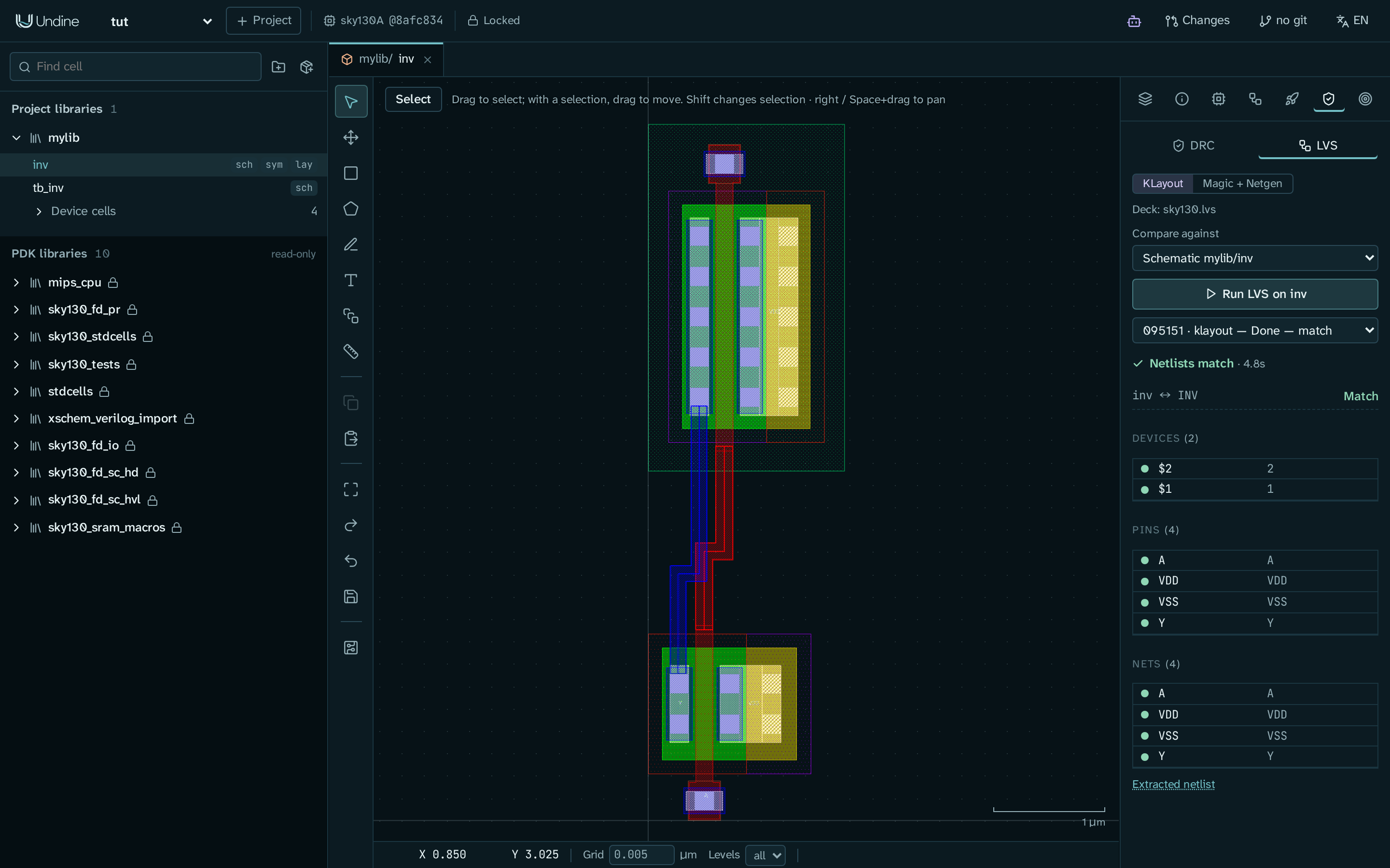
- In the layout's side panel, open DRC / LVS (the shield icon). On the DRC tab, with KLayout chosen, click Run DRC on inv. After a few seconds you should see No violations (256 rules).
- Open the LVS tab. Compare against is Schematic invlib/inv. Click Run LVS on inv. You should see
Netlists match,
inv ↔ INVMatch, and the two devices, four pins and four nets matched. - Optionally, choose Magic on the DRC tab and Magic + Netgen on the LVS tab and run them too: the same tools that shuttle prechecks use. Both should agree (No violations; Circuits match).
If DRC reports poly.1a
poly.1a (minimum poly width) at the end of your poly path means the path is a few nanometres off the gate's
centre line, which leaves a sliver narrower than 0.15 µm. Select the path, press Del, set the grid to 0.01
and draw it again. Click a violation in the list to see its marker in the layout.
If LVS does not match, the result says where: a device or pin without a counterpart, or a net with too few connections. A missing label is the most common cause. Verification explains the reports.
11. Check the whole cell
The cell page collects every check of the cell. To have them all on the design as it is now:
- In the layout's side panel, open Tapeout: shuttle checks and bundle (the rocket icon).
-
Under Sign-off suite, click Run all checks (KLayout, Magic, Netgen). If some results from step 10 are still current, the button reads Run N outdated or missing checks instead and runs only the others. The suite covers the KLayout DRC decks, Magic DRC, KLayout LVS and Magic + Netgen LVS. When they are done, the panel says Every check ran on the design as it is now and passed.
The Layout checks above the suite are for a shuttle's top cell (a Tiny Tapeout tile, a die). A bare inverter fails them; ignore them here.
-
Open the cell page of
invagain (click its name in the library browser). It now reads In invlib. Its schematic, symbol, and layout agree. Its checks pass.The Layout row says Devices match the schematic., the testbench row shows its last simulation as current, and below the waterline (Generated from the views above) every check is Clean or Matched and current.
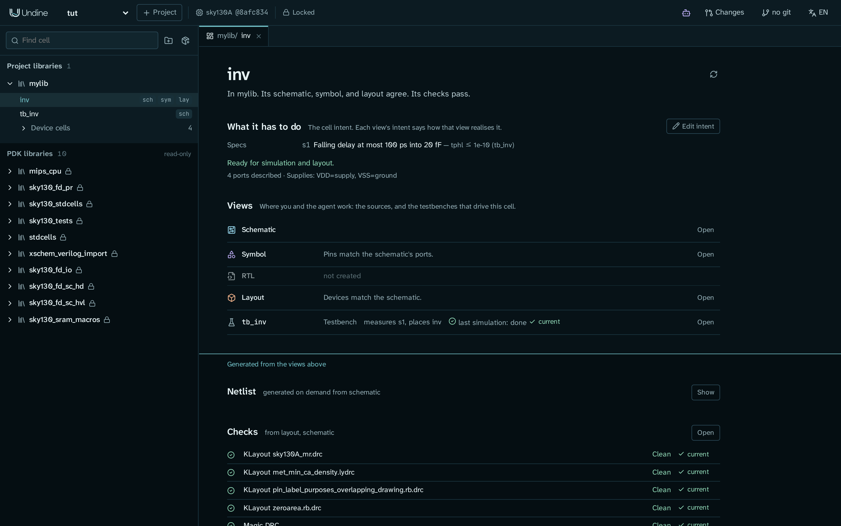
Every result remembers what it ran on. Change the design and the result is marked outdated with what changed, for example layout of invlib/inv changed, until you run it again; undo the change and it is current again.
Try it: in the inv schematic, set W of M2 to 1.5. The cell page says the layout is out of date
(devices out of date with the schematic: M2). Then press Ctrl+Z in the schematic (or set W back to 1), and
the cell page is current again. Do not click Update layout in the Schematic-driven layout panel here: it swaps
in the new PCell, but it does not redo your routing. Outdated results
explains what each result depends on.
What you learned
- A cell has views (schematic, symbol, layout) and a design intent; the cell page shows how they stand together.
- The schematic is the source of the netlist, the symbol and the layout's devices; a testbench is another schematic that places the cell.
- A spec says what to measure, on which testbench, and the limit;
check_specsmeasures it. - Schematic-driven layout places the devices; you route the nets and label the pins, and LVS confirms the result.
- Every check and simulation records its inputs, so an outdated result is flagged instead of trusted.
Next steps
- Design with an AI agent: let an agent size and verify a cell from its intent, and review its changes.
- Tape out on Tiny Tapeout: put an inverter like this one in a Tiny Tapeout analog tile and export
the bundle. That tutorial rebuilds the inverter with the example scripts in
mylib, so your hand-routed layout ininvlibstays as it is. - Layout editor, Schematic editor and Verification: the full reference for each step.
- Changesets: propose edits, review them and adopt or discard them.