First project
This page is a quick tour of Undine. You create a project, start the server, build the demo designs with the example scripts, and look at them in the browser: the library browser, a cell page, a schematic, a layout and a simulation. At the end you know where everything is, on screen and on disk.
You do not draw anything here: the scripts build a CMOS inverter, its testbench, its routed layout and a Tiny Tapeout tile around it. Your first cell: an inverter is where you draw a cell yourself.
The tour takes about 15 minutes, most of it reading.
Before you start
You need:
- Undine installed, with the sky130A PDK. See Install.
./setup.sh check(orpixi run doctor) tells you what is missing. - A terminal in your checkout of Undine. The examples on this page use
~/undine-eda. - A web browser on the same machine.
1. Create a project
A project is a directory that holds your libraries and cells, pinned to one exact version of a PDK. Create one named
demo on sky130A:
cd ~/undine-eda
pixi run python -m undine new demo --pdk sky130A
You should see:
created /home/you/undine-projects/demo (pdk sky130A@8afc8346a57f)
--pdk sky130A picks the installed version of sky130A that Undine is tested with, and the project records that exact
version (sky130A@8afc8346a57f) in its project.json. The project keeps it until you move it on with set-pdk
(Command line and configuration), so the design simulates and verifies the same way months later.
Where projects are kept
Projects live in ~/undine-projects by default. To keep them elsewhere, set UNDINE_ROOT
(for example export UNDINE_ROOT=~/chips) in every terminal you use for Undine: the server and the example scripts
must see the same directory. See Configuration.
2. Start the server
Undine is a server: the design database, the PDK, the PCells, DRC / LVS and simulation all run in it, and the browser only draws. Start it:
pixi run serve
It prints one line and then keeps running:
undine: 2 PDKs, projects in /home/you/undine-projects
The number of PDKs depends on what you installed (setup.sh installs sky130A and sky130B). Leave this terminal open;
the server runs until you press Ctrl+C there. Open a second terminal for the commands of the next steps.
The port is taken?
pixi run serve listens on 127.0.0.1:8700. If another program (or another Undine) already uses that port, start
this one on another: pixi run python -m undine serve --port 8701, and use that port in the addresses below.
3. Open Undine in your browser
Open http://127.0.0.1:8700 in a browser on the same machine.
Windows with Undine in WSL
Open the address in your Windows browser. WSL2 forwards 127.0.0.1 from Windows to the server inside WSL.
You should see the Undine window. Select demo in the project menu at the top left if it is not selected already
(the window opens the first project of the list). The left side, the
library browser, lists only PDK libraries (marked read-only): the PDK's device symbols (sky130_fd_pr), its
standard cells and its other Xschem libraries. Your project has no library of its own yet.
Creating a project in the browser
The + Project button next to the project menu creates a project like step 1: it opens New project, where you give a Name and choose the PDK, pinned to this exact version, then click Create. When several versions of a PDK are installed, check that the version in the list is the one you want.
4. Build the demo designs
In the second terminal, still in ~/undine-eda, run the three example scripts in this order:
pixi run python examples/make_inverter.py demo mylib     # inverter schematic, symbol and testbench
pixi run python examples/route_inverter.py demo mylib    # the inverter's layout, routed, then LVS
pixi run python examples/make_tt_inverter.py demo mylib  # a Tiny Tapeout tile around the inverter
The first two arguments are the project and the library. The library mylib is created when it does not exist.
| Script | What it builds | What you should see |
|---|---|---|
make_inverter.py |
the cell inv (schematic and symbol: a PMOS and an NMOS, ports A, Y, VDD, VSS) and the testbench tb_inv |
three lines wrote .../libs/mylib/inv.sch, inv.sym, tb_inv.sch |
route_inverter.py |
the layout of inv: its transistors generated from the schematic as PDK PCells, then routed by hand through the Design API; then it runs LVS |
after about 30 seconds, done {"match": true, ...} and the devices, pins and nets of the comparison, each Match |
make_tt_inverter.py |
tt_um_undine_inv, a 1x2 Tiny Tapeout analog tile with the inverter wired from ua[0] to ua[1] |
nothing; it returns after about 40 seconds |
make_inverter.py writes the files directly. The other two also work through the running server, so the server from
step 2 must be running, on the same machine and with the same UNDINE_ROOT: they read and write some of the
project's files themselves. The scripts are safe to run again: each one rebuilds its cells from scratch.
Server on another port
route_inverter.py and make_tt_inverter.py take the server's address as a third argument, for example
pixi run python examples/route_inverter.py demo mylib http://127.0.0.1:8701.
Leave out pixi run
pixi shell opens a shell with Undine's environment active; in it you can leave out the pixi run prefix
(python -m undine serve, python examples/make_inverter.py demo mylib).
Now reload the page in your browser (F5). The library browser has a new group, Project libraries, with
mylib. Click mylib to expand it if it is not open. You should see:
tt_um_undine_inv(sch,lay): the Tiny Tapeout tile, highlighted as a top cell (no other layout cell places it);inv(sch,sym,lay): the inverter;tb_inv(sch): its testbench;- Device cells (8): the PCell cells generated for the layout (transistors and vias), folded into one row.
5. Take a tour of the window
Your editor area is still empty: no cell is open yet. Once you have opened the inverter in steps 6 to 8, the window looks like this:
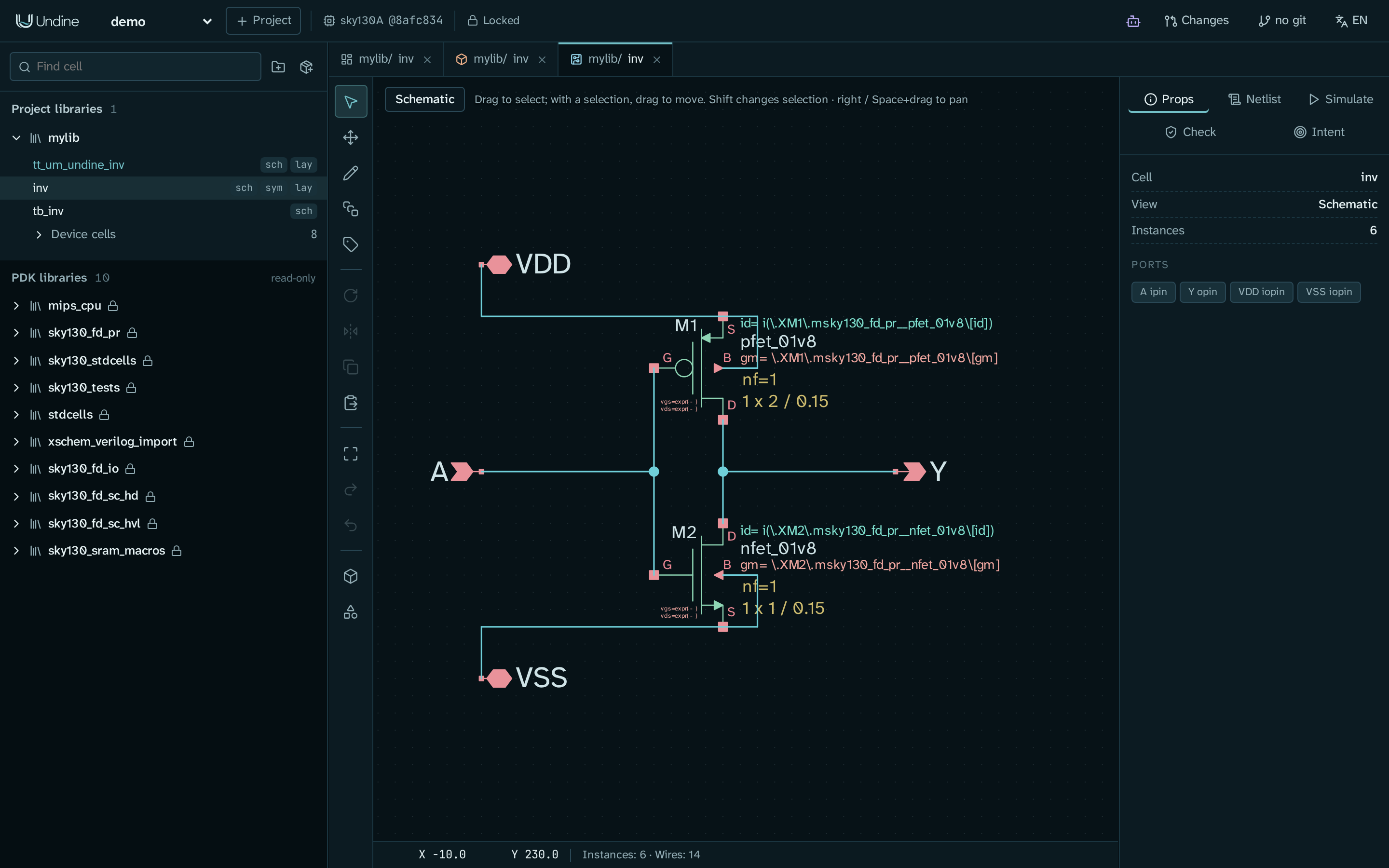
Top bar, from left to right:
| Item | What it does |
|---|---|
Project menu (demo) |
switches between your projects |
| + Project | creates a project |
PDK badge (sky130A @8afc834) |
the PDK version the project is pinned to; click it for how it stands against undine.lock, Fetch... when it is missing, and Rescan PDKs (PDKs) |
| Locked | the PDK and the dependencies match undine.lock; otherwise it shows the number of lock issues. A tool of another version is a warning listed in its dialog, not a lock issue (Libraries and dependencies) |
| Agent button (robot icon) | shows or hides the in-app Agent panel, where you ask an AI about the design or give it work (Agent and MCP) |
| Changes | opens the list of changesets: proposals (from an agent, or your own) that you review, then adopt or discard (Changesets) |
| git button (no git, or the branch name) | opens the History panel: commits and uncommitted changes, cell by cell (Git history) |
| Language menu (EN / JA) | switches the interface between English and Japanese (Interface language) |
Library browser (left). Find cell filters the cells of all libraries by name. The buttons next to it, and those of each library of your own, create libraries and cells (Start a design of your own). In a cell's row:
- click the name to open the cell's cell page;
- click
sch,sym,rtlorlayto open that view directly.
Editor tabs (middle). Each view you open gets a tab, labelled with the library and the cell and an icon for the
view. The browser remembers the open tabs of each project. A link of the form
http://127.0.0.1:8700/#/p/demo/o/mylib/inv/schematic opens one view directly (the last part can be cell,
schematic, symbol, rtl or layout), which is handy for a bookmark.
Side panel (right). Each editor has its own side panel. The schematic editor's has the tabs Props, Netlist, Simulate, Check and Intent; the layout editor's has icon tabs, whose names show when you point at them: Layers, Properties, PDK PCells, Schematic-driven layout, Tapeout (rocket), DRC / LVS (shield) and Intent.
6. Open the inverter's cell page
Click the name inv in the library browser. The cell page opens:
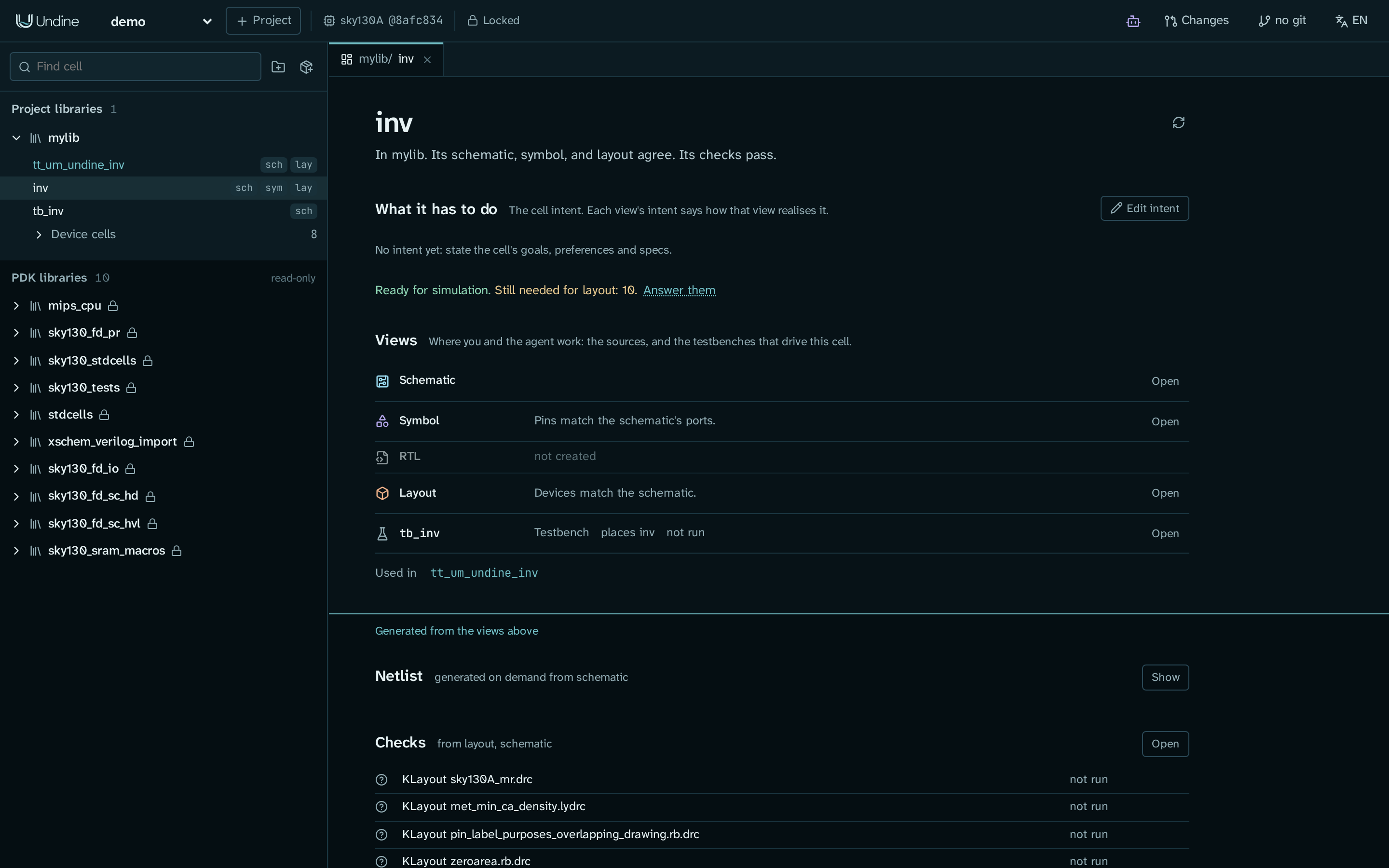
From the top:
- the cell's name and a sentence on where it stands: In mylib. Its schematic, symbol, and layout agree. Its checks pass.
- What it has to do: the cell's design intent (goals, specs, constraints). The demo has none yet: No intent yet. Edit intent opens the editor. Below it, a line says what the intent still lacks before each step (Ready for simulation. Still needed for layout: 10.); Answer them opens those questions. You can leave them for now.
- Views: the schematic, the symbol (Pins match the schematic's ports), RTL (not created), the layout (Devices
match the schematic) and the testbench
tb_inv(not run, until you simulate it in step 9). Open opens each one. Used in names the cells that placeinv:tt_um_undine_inv. - Below the aqua line, the waterline, is what is generated from the views: the Netlist (Show) and the
Checks. KLayout LVS says Matched and current: that is the LVS run
route_inverter.pymade, on the layout as it is now. The DRC decks say not run.
Cells, intent and views explains the cell page and design intent in full.
7. Open the schematic
Click sch in the row of inv (or Open next to Schematic on the cell page). You see the inverter: the PMOS
M1 above, the NMOS M2 below, the ports A, Y, VDD and VSS.
- Click
M2. Props shows its symbol (sky130_fd_pr/nfet_01v8.sym) and its attributes:W,L,nf... - Click the Netlist tab. It shows the SPICE netlist of the cell, with
XM1andXM2and their sizes (W=2andW=1,L=0.15). - Press F to fit the drawing to the window. Scroll to zoom; drag with the right mouse button (or Space+drag) to pan.
Schematic edits are saved at once
The schematic editor writes each edit to the .sch file immediately (Undo takes it back). Feel free to try things
on the demo; make_inverter.py builds it again.
The keys and tools are in the Schematic editor guide.
8. Open the layout
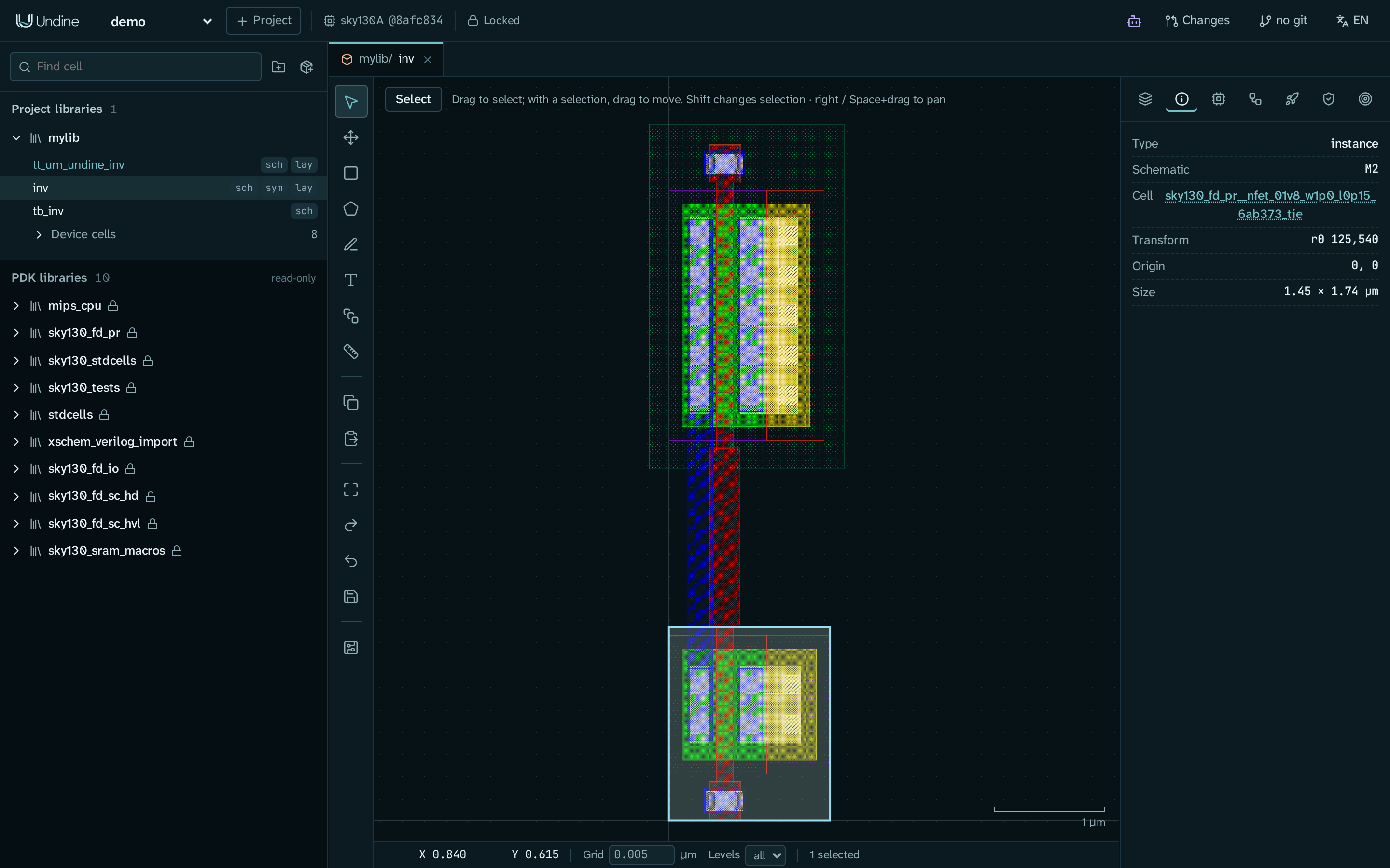
Click lay in the row of inv. The layout shows the PMOS above the NMOS, joined by a poly gate and routed on li1 and
met1. The layers come from the PDK; the Layers tab lists them.
- Click the lower transistor, then the Properties tab (the i icon). It shows an instance of a generated PCell
cell, and Schematic
M2: the layout knows which schematic device it was generated from. - Press F to fit. Scroll to zoom; drag with the middle or right mouse button to pan.
- Double-click an instance to open its cell in a tab of its own.
Layout edits wait for a save
Unlike the schematic editor, the layout editor does not write each edit to the cell's .oas file. With a
selection, a left drag moves it, so a stray drag is an edit too. Press Ctrl+S (or the save button in the
toolbar on the left of the drawing) to write the cell files; until then the edits are kept in the operation log on
the server, and they survive a restart. Undo (U or Ctrl+Z) takes an edit back.
The DRC / LVS tab (shield icon) runs DRC and LVS on this cell. Now open the tile: click lay in the row of
tt_um_undine_inv and zoom out to see the whole 1x2 tile with its met4 pins and power stripes; the inverter sits near
the bottom right. The Layout editor and Verification guides cover drawing,
schematic-driven layout, DRC and LVS.
9. Run a simulation
The testbench tb_inv drives the inverter with a 1.8 V supply, a pulse on the input and a 20 fF load, and its code
block runs a 20 ns transient analysis with the sky130 models at the typical corner.
- Click
schin the row oftb_inv. - In the side panel, click Simulate.
- Leave Analysis at Use commands in the schematic and click Run ngspice.
The run appears under Jobs with a tick when it is done (a second or two). Below it, the plot, headed Transient
Analysis, shows the first node voltages, v(in), v(out) and v(vdd): the output switches each time the input
does. Scroll on the plot to zoom in on an edge, double-click to reset. Tick and untick signals in the list under the
plot (Filter signals narrows it).
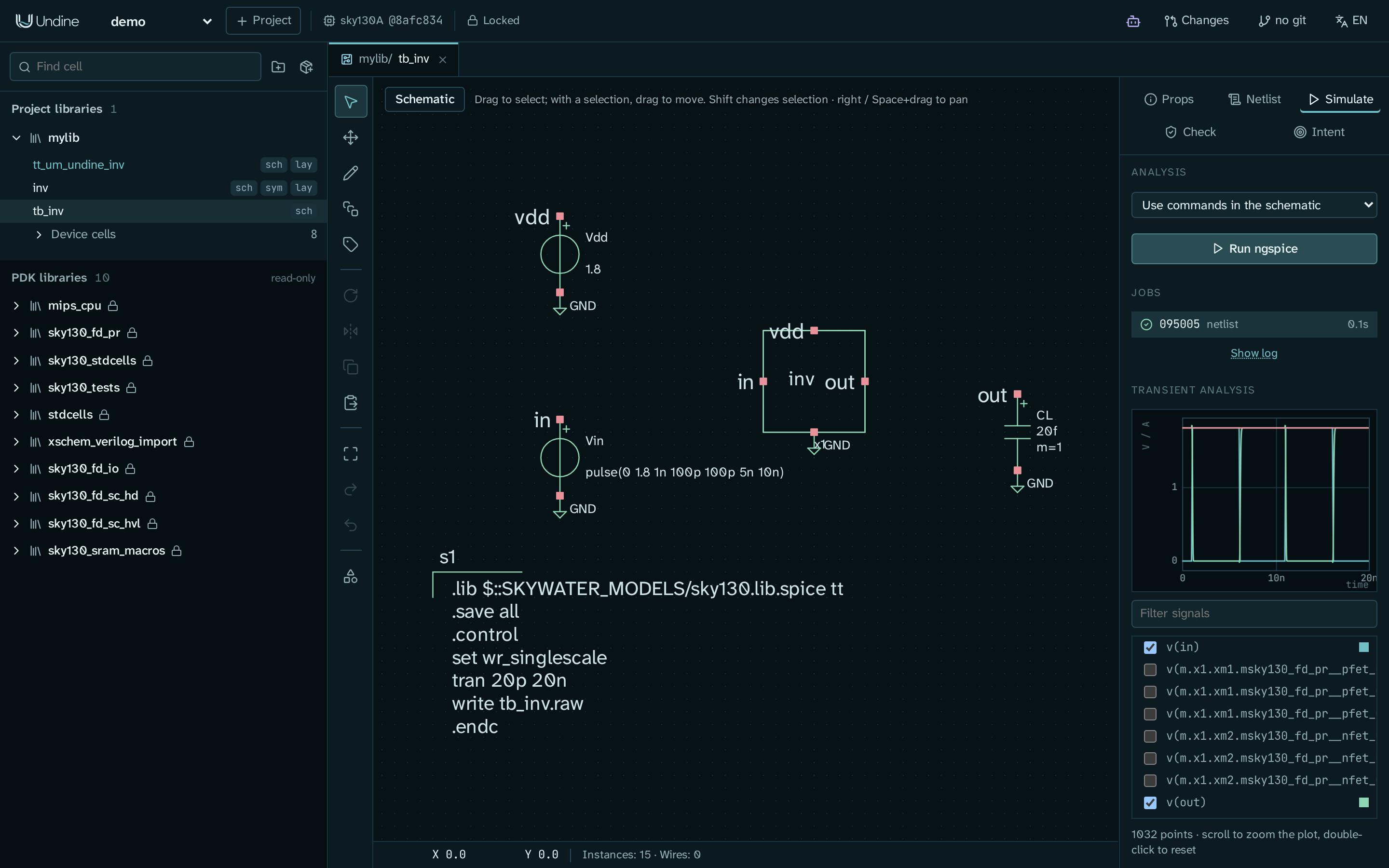
ngspice runs on the server, not in the browser. Go back to the tab of the cell page of inv: the row of tb_inv now
says last simulation: done and current. The Schematic editor guide covers the other
analyses (AC, DC sweep, operating point); Verification covers specs measured at corners,
post-layout simulation and sweeps.
10. Find your files on disk
Everything Undine knows about the project is in its directory, as ordinary files:
~/undine-projects/demo/
    project.json          the project: its name, the pinned PDK, its libraries
    undine.lock           the PDK and tool versions the project is locked to
    libs/mylib/
        inv.sch, inv.sym  the schematic and the symbol, in Xschem format
        inv.netlist.yaml  the schematic's netlist view (its connectivity)
        inv.oas           the inverter's layout (OASIS), one file per cell
        tb_inv.sch, tt_um_undine_inv.sch, tt_um_undine_inv.oas, ...
    history/mylib.jsonl   the operation log: who changed what, and why
    runs/<job>/           each simulation, DRC and LVS run: inputs, netlists, logs, results
    changesets/           the changesets and what they leave behind
Xschem can open libs/mylib as it is. KLayout can read the .oas files too, but each file holds one cell and names
the cells it places without their contents: load all of a library's files into one layout to see the whole hierarchy
(Layout cell files). The full layout, with the files of changesets, tapeout
bundles and the agent, is in Data layout.
11. Put the project in git
Changesets, the proposals you review in the agent tutorial, are git branches, so put the project in git now.
- If you changed a layout in step 8, save it first (Ctrl+S in its tab). Set up git makes no first commit while a layout has unsaved edits.
- Click the git button, which says no git. The History panel opens.
- Click Set up git, and confirm in the dialog.
Undine runs git init, adds a .gitignore and .gitattributes, registers its diff and merge drivers and commits the
project's files as the first commit. The button then shows the branch name. See Git history.
12. Stop the server
Press Ctrl+C in the terminal where the server runs. Schematic edits are already in their files; save any layout you
changed (Ctrl+S) before you stop, although unsaved layout edits are kept in the operation log and come back after a
restart. Start the server again with pixi run serve whenever you need it. A simulation that is still running carries
on and the next server takes it up (Restarting the server).
Start a design of your own
When you are ready to work on your own cells:
- A new library: the folder button at the top of the library browser (New library).
- A library dependency: the package button next to it (Add library dependency): a library from a git repository, pinned to a commit (Libraries and dependencies).
- A new cell: the + button of a library (New cell): a name and the views to create (schematic, symbol, RTL, layout).
-
An existing cell: the import button of a library (Import existing cell): an Xschem
.schor.sym, or a.gds,.oasor.oasislayout, from a path on the server. The path must be inside your home directory by default (serve --import-root DIRallows other directories; see Command line and configuration). A layout can also be imported from the command line:pixi run python -m undine import demo mylib chip.gds
What you learned
- A project is a directory under
~/undine-projects(UNDINE_ROOT), pinned to an exact PDK version. - The server does the work (database, PDK, PCells, checks, simulation); the browser at http://127.0.0.1:8700 draws.
- The library browser opens a cell's cell page (click the name) or one of its views (
sch,sym,rtl,lay). - The cell page shows whether a cell's views agree and how its checks and simulations stand.
- Simulations run with Simulate → Run ngspice in a testbench's schematic.
- Your design is plain files: Xschem schematics and symbols, OASIS layout cells, YAML netlists and an operation log.
Next steps
Tutorials:
- Your first cell: an inverter: draw the schematic, simulate it and build the layout yourself.
- Design with an AI agent: write down a cell's intent, let an agent size the cell, then review and adopt its proposal.
- Tape out an analog tile on Tiny Tapeout: take
tt_um_undine_invthrough the shuttle's checks, the sign-off suite and the export bundle. - Case study: an 11-bit SAR ADC: a full mixed-signal design built in Undine.
To connect Claude Desktop, Claude Code or another AI app, follow Connect an AI agent.
The User guide covers each editor and workflow in depth; the pages this tour pointed to are Cells, intent and views, the Schematic editor, the Layout editor, Verification, Changesets and Git history. The Reference, starting with Command line and configuration, lists every command and setting.